Block diagram & Pin description
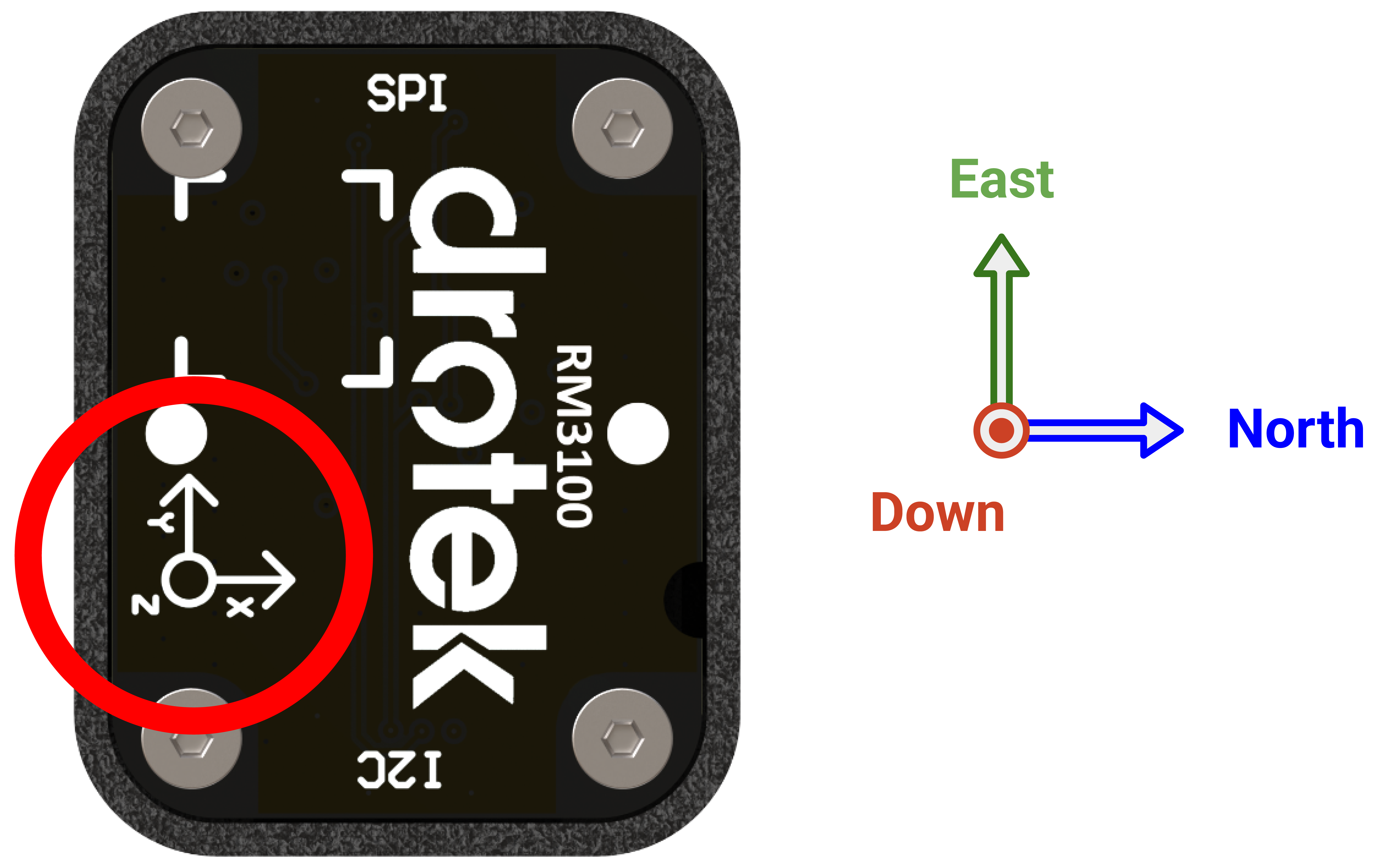
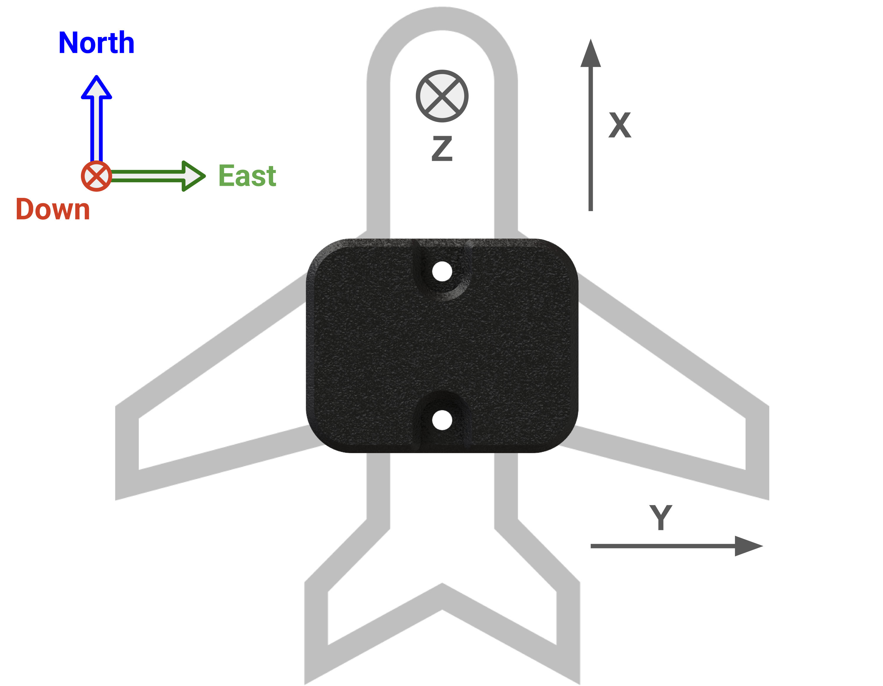
ORIENTATION
PIN DESCRIPTION
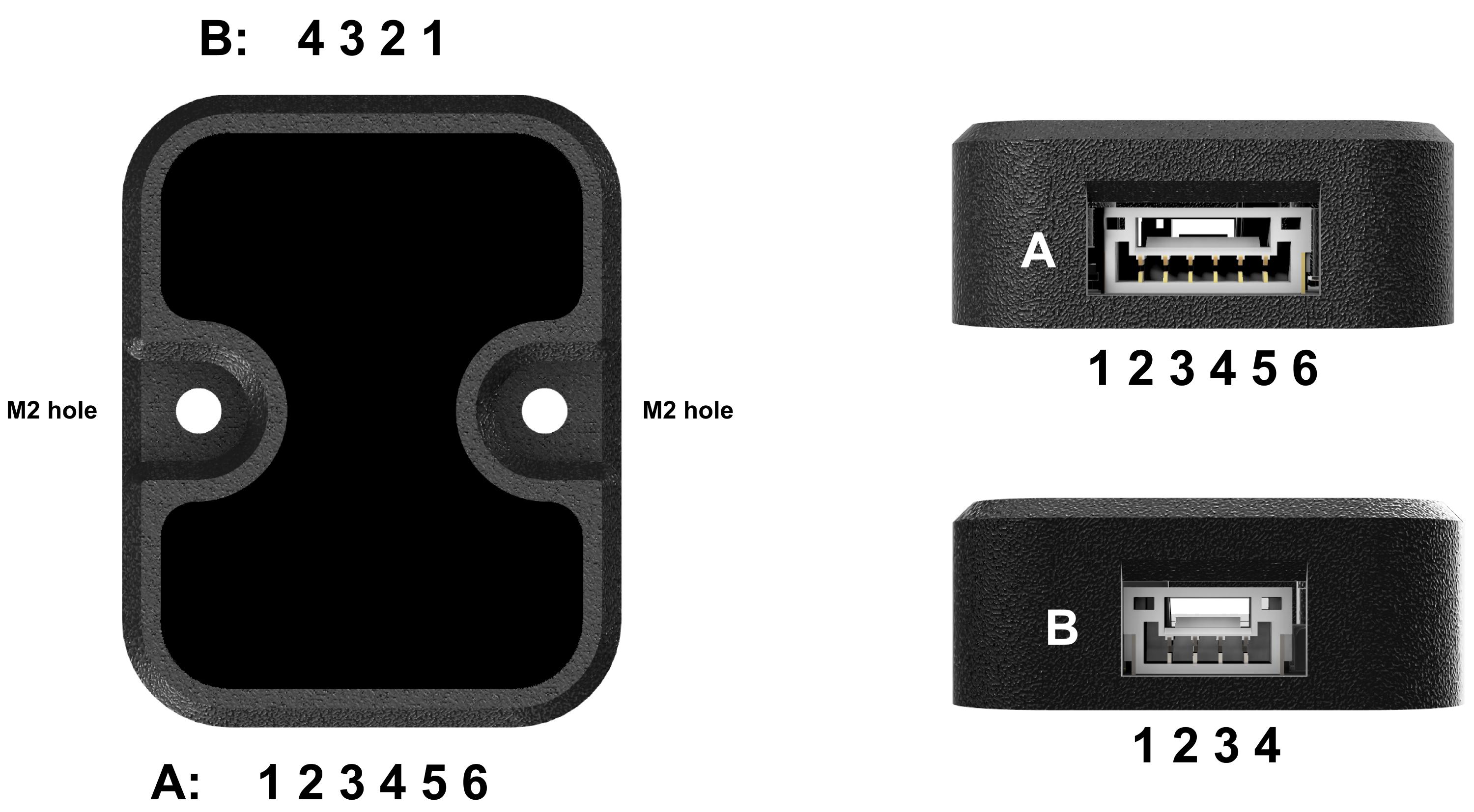
| Pin | Name | Type | Function |
|---|---|---|---|
| A1 | 5V IN | P | 5V Input |
| A2 | SPI SCK | I | SPI Clock |
| A3 | SPI MISO | O | SPI Master Input, Slave Output |
| A4 | SPI MOSI | I | SPI Master Output, Slave Input |
| A5 | SPI CS | I | SPI Chip Select |
| A6 | GND | P | Ground |
| Pin | Name | Type | Function |
|---|---|---|---|
| B1 | 5V IN | P | 5V Input |
| B2 | I2C SCL | I | I2C Serial Clock |
| B3 | I2C SDA | I/O | I2C Serial Data |
| B4 | GND | P | Ground |
Electrical specifications
| Symbol | Parameter | Min. | Typ. | Max. | Units |
|---|---|---|---|---|---|
| Vin | 5V input | 4.5 | 5.0 | 5.5 | V |
| Vdd | Internal voltage | 3.3 | V | ||
| Vdd_IO | IO voltage | 3.3 | V | ||
| Idd | 1 | 10 | mA | ||
| Vil | I/O low level input volt | 0 | 0.3*Vdd | V | |
| Vih | I/O high level input volt | 0.7*Vdd | Vdd | V | |
| Top | Operating Temperature | -40 | +85 | °C |
RM3100 specifications
| Parameter | 50 CC | 100 CC | 200 CC | Units |
|---|---|---|---|---|
| Field Meas. Range | -800 to 800 | -800 to 800 | -800 to 800 | µT |
| Gain | 20 | 38 | 75 | LSB/µT |
| Sensitivity | 50 | 26 | 13 | nT |
| Noise | 30 | 20 | 15 | nT |
| Noise Density | 1.2 | 1.2 | 1.2 | nT/√Hz |
| Repeatability over ±200µT | 15 | 8 | 8 | nT |
| Hysteresis over ±200µT | 15 | 15 | 15 | nT |
| Linearity over ±200µT | 0.5 | 0.5 | 0.5 | % |
| Max Sampling Rate | 1600 | 850 | 440 | Hz |
RM3100 7bit I2C address: 0b0100000 (0x20)
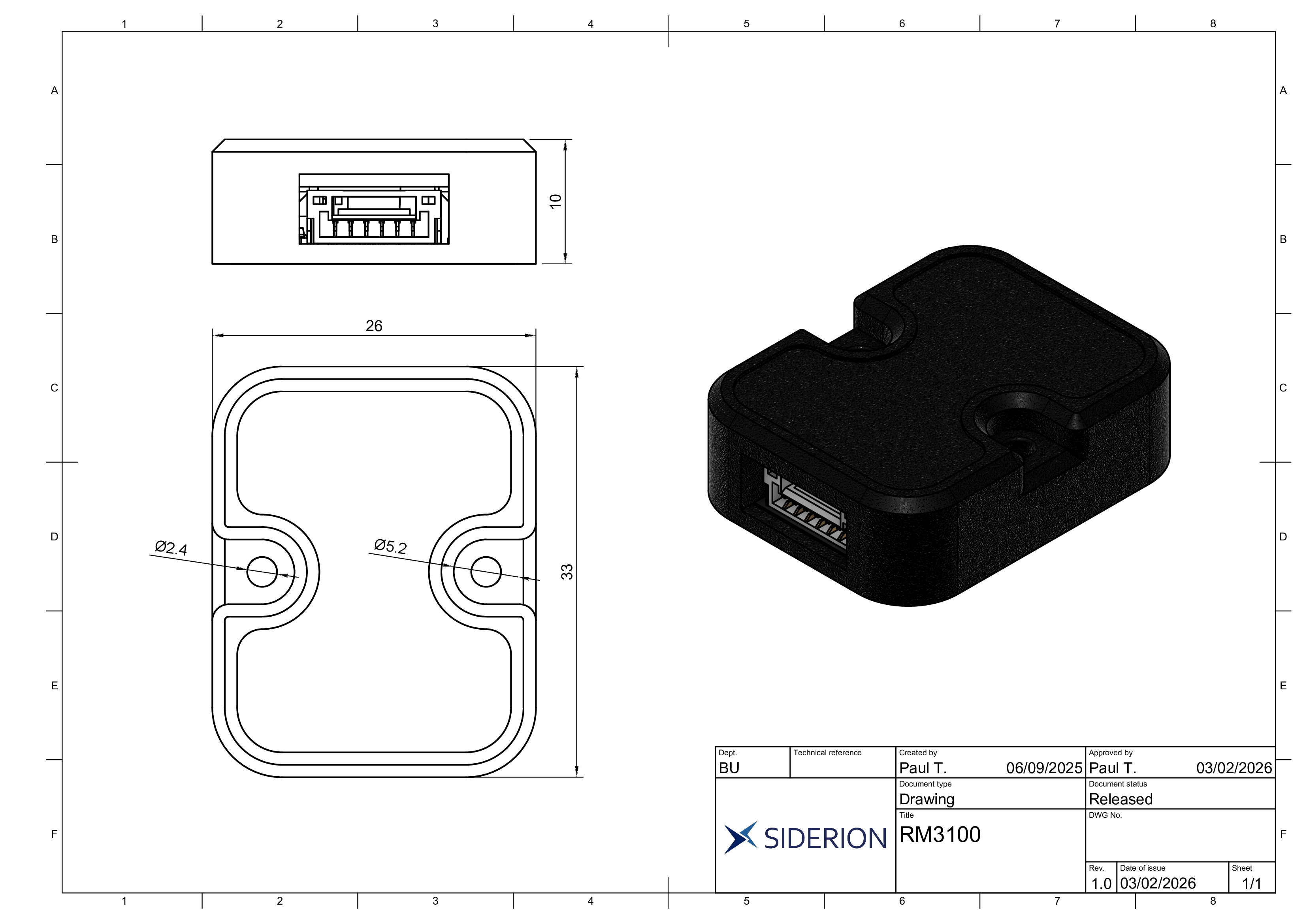
Mechanical